PC4-5
Observability of anomalous metal state of atomic layer superconductors NbSe2 in transport measurement
*Akinobu Kanda1, Riki Yanai1, Liang Haoyun1, Masato Ishikawa1, Hikari Tomori1, Kenji Watanabe2, Takashi Taniguchi2, Masahiko Hayashi3
- Department of Physics, University of Tsukuba, Japan1
- NIMS, Japan2
- Faculty of Education and Human Studies, Akita University, Japan3
Condensed matter physics textbooks of graduate level tell that in two dimensional (2D) systems, no metallic state survives at zero temperature due to Anderson localization.[1] This notion has been confirmed, e.g., through observation of the weak localization effect in transport measurements.[2] On the other hand, in recent years, intensive studies on ultraclean 2D superconducting materials, obtained by mechanical exfoliation, MBE and so on, have experimentally revealed the existence of the anomalous metallic state, in which the resistance saturates to a finite value in magnetic fields even in the zero-temperature limit.[3]
The anomalous metallic state has been attributed to the quantum phase fluctuations that prevent the global phase coherence. Theoretically, quantum fluctuations are suppressed by introducing dissipation, and dissipation-driven suppression of quantum fluctuations was experimentally observed in Josephson junction arrays,[4] in which each Josephson junction was shunted by a lithographically defined micrometer-sized Cr resistor. Similar attempt was carried out for 2D superconductors,[5] and restoration of zero-resistance state was observed. Note, however, that in ref.[5], the source of dissipation is a conventional resistor inserted between the voltage source and the sample in series, while in ref.[4], the resistor was made on the sample substrate and close to the junction. It is not clear whether the resistor in ref. [5] really removed quantum fluctuations, or just worked as a lowpass filter. Actually, it is reported that the 2D superconductivity are so weak that the external noise suppresses superconductivity, leading to the finite resistance (anomalous metallic) state, unless the cryostat is properly filtered.[6] Thus, the origin of the anomalous metallic state is unclear.
Here, we point out another origin of the anomalous metallic behavior, which is related to nonlinear current-voltage characteristics. We stress that careful measurement is required for the accurate estimation of zero-bias resistance.
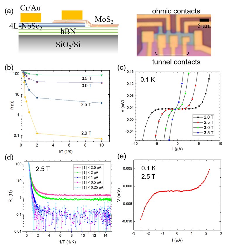
Our sample is a four-layer 2H-NbSe2 which is sandwiched between hBN and MoS2 layers, as shown in Fig. (a). This stacking structure was made in a glove box filled with inert gas. The superconducting transition temperature is Tc = 6.3 K, at which the resistance becomes 50% of the normal state resistance. This value agrees with the literature values. The residual resistance ratio (RRR) was 7. We observed Kosterlitz-Thouless transition of vortices with the transition temperature TKT = 5.7 K, which was determined from the square-root-cusp behavior of resistance and the universal jump in the power-law behavior of the current-voltage characteristics. These results indicate that the quality of our sample is similar to those in the literature.
Figure (b) shows the zero-bias resistance R at several temperatures for perpendicular magnetic fields B = 2.0 T, 2.5 T, 3.0 T, and 3.5 T in the Arrhenius (log R – 1/T) plot. Zero-bias resistance was calculated from the linear fit of current-voltage (I-V) characteristics in the current range |I| < 3.5 mA. This figure is quite similar to Fig. S3(a) in ref.[3] for 4L-NbSe2, which reports anomalous metallic (quantum metallic) behavior. However, as shown in Fig. (c), for B = 2.5 T, 3.0 T, and 3.5 T, the I-V characteristics at 0.1 K (1/T = 10 [1/K]) is nonlinear in the used current range of |I| < 3.5 mA, so that the resistance values are not accurate at low temperatures. Besides, as explained below (Fig. (d)), the resistance at 2.0 T in the low temperature range is near or below noise floor. To see behavior of the derived resistance in more detail, we measured detailed I-V characteristics for B = 2.5 T, as shown in Fig. (e). Here, there are 100 data points for each I-V curve. Figure (d) shows zero-bias resistances calculated from the data points in the current range |I| < 2.5, 2, 1, 0.5 and 0.25 μA. The zero-bias resistance decreases as the current range shrinks, and finally it becomes under the noise floor (R < 0.3 Ω), showing that the sample is in the zero-resistance state. From these measurements, we can conclude that one needs to keep the biasing current as small as possible to detect a metallic state accurately.
[1] Y. Nagaoka, Prog. Theor. Phys. Supp., 84, 1 (1985).
[2] S. Kobayashi, F. Komori, Y. Ootuka, and W. Sasaki, J. Phys. Soc. Jpn, 49, 1635 (1980).
[3] For example, A. Tsen, B. Hunt, Y. Kim, et al., Nat. Phys. 12, 208 (2016).
[4] T. Yamaguchi, R. Yagi, A. Kanda, Y. Ootuka, and S. Kobayashi, Phys. Rev. Lett. 85, 1974 (2000).
[5] A. Banerjee, A. Mohapatra, R. Ganesan, and P. S. Anil Kumar, Nano Lett. 19, 1625 (2019).
[6] I. Tamir, A. Benyamini, E. J. Telford et al., Sci. Adv. 5, eaau3826 (2019).
Figure captions:
(a) Schematic side view and optical image of the sample. (b) Temperature dependence of zero-bias resistance, which is calculated from the I-V curve in |I| < 3.5 μA. (c) I-V curves for the resistance calculation in (b). (d) Temperature dependence of zero-bias resistance, which is calculated from the I-V curve in several current ranges. (e) I-V curve for the resistance calculation in (d).
Keywords: 2D superconductivity, anomalous metal state, quantum metal state, transport measurement