PC4-7
Vortex penetration and expulsion in mesoscopic-sized atomically thin superconductor NbSe2
*Haoyun Liang1, Riki Yanai1, Hikari Tomori1, Takashi Taniguchi2, Kenji Watanabe2, Masahiko Hayashi3, Akinobu Kanda1
- Department of Physics, University of Tsukuba, Japan1
- NIMS, Japan1
- Faculty of Education and Human Studies, Akita Unicersity, Japan1
In mesoscopic superconductors, which contain structures with sizes comparable to or smaller than the superconducting coherence length or the magnetic penetration depth, the quantum confinement of supercurrent dramatically modifies superconducting properties. Notably, carefully nano-engineered superconductors are expected to bring out outstanding properties that are never seen in conventional bulk superconductors, and have a possibility of novel application to quantum technology.
So far, we have investigated such superconducting states in mesoscopic aluminum (Al) superconductors using our original small tunnel junction method. In this method, superconducting states, especially vortex arrangement, were detected using the transport properties of the small tunnel junctions attached to edges of the superconductor. Local tunnel spectroscopy allows one to investigate continuous variation of the superconducting density of states as a function of magnetic fields, current, temperature and so on. We have succeeded in confirming the existence of mesoscopic superconducting states such as giant vortex states and manipulating vortex locations by current injection.
Here, we apply our technique to atomically thin superconductors. Owing to the micromechanical exfoliation of layered materials and dry stacking of arbitrary layered materials developed in the 2D materials research, one can obtain atomically thin and clean superconductors. In such superconductors, novel superconducting states such as Bose metal has been observed, instead of the superconductor-to-insulator quantum phase transitions in disordered films. On the other hand, to our knowledge, mesoscopic superconducting properties in 2D superconductors have never been studied.
Here we focus on 2D superconductor NbSe2 with mesoscopic size and discuss the difference between NbSe2 and aluminum in the behavior of the vortex observed by the small tunnel junction method. In our sample, a cleaved film MoS2 and Ti/Au are used as tunnel barrier and normal conductor, respectively.
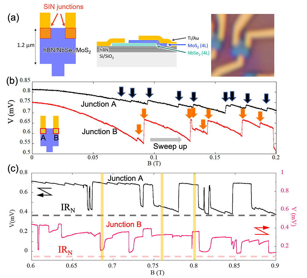
In sample fabrication, we first stacked 4-layer NbSe2 and 4-layer MoS2 on an hBN flake placed on a silicon substrate using the dry-transfer method. The stacking process was carried out in a glove box filled with inert gas. Next, Ti/Au electrodes were connected to the stacked structure by electron beam lithography and lift-off. Finally, the stacked structure was etched into a rectangular shape by reactive ion etching. Figure (a) shows schematic plane and cross-sectional views and an optical image of the sample. The mesoscopic superconductor size of the sample is (1.2 μm)2, and two tunnel junctions with area of (0.35 μm)2 is attached to corners of the sample, as shown in Fig. (a).
The current-voltage (I-V) characteristics were measured at 0.1 K, and the differential conductance (dI/dV) was calculated from the I-V characteristics. The superconducting gap estimated from the dI/dV-V curve is 0.94 meV, which agrees with the literature value for 4L-NbSe2. In the small tunnel junction measurement, we fixed the current flowing through each tunnel junction to 20 pA and measured the tunnel junction voltages as a function of the perpendicular magnetic field.
Figures (b) and (c) show the magnetic field dependence of the junction voltages in the low magnetic field region of 0 - 0.2 T and the medium magnetic field region of 0.6 - 0.9 T, respectively. The black line corresponds to junction A and the red line to junction B.
In Fig. (b), the voltage jumps at different positions for junctions A and B, respectively. The jump interval is about a few tens of mT, which is several to several tens of times larger than the 1.4 mT interval of the magnetic field, corresponding to the magnetic flux quantum. This vortex behavior suggests that dozens of vortices are penetrating at the same time. In the case of aluminum, the voltage jumps in each of the four tunnel junctions occur simultaneously, and the jump intervals are in good agreement with the magnetic fields corresponding to the magnetic flux quantum.
Figure (c) shows the field dependence of the junction voltage in the medium field region of 0.6-0.9 T. The dotted lines represent the voltage at normal conduction IRN for junctions A and B, respectively. Both junctions A and B show high voltage jumps, and the voltage values on the low voltage side of the jumps are close to IRN. Such a drastic change in junction voltage is not seen in aluminum. We observed the gap structure in the magnetic field shaded in yellow in figure (c) to confirm the change in superconductivity in the medium field region. At 0.68 T, where junction B exhibits a lower voltage, superconductivity is unchanged at junction A and weakened at junction B. Conversely, at 0.76 T, where junction A exhibits a lower voltage, superconductivity weakens at junction A and does not change at junction B. At 0.8 T, where the voltage value of both junction A and B is high, superconductivity is maintained in both junctions. These results suggest that the superconductivity weakens dramatically in the region where the voltage drops sharply.
In the presentation, we will discuss the difference in superconducting properties between NbSe2 and aluminum in detail.
Figure captions:
Figure: (a) Sample structure, cross section, and optical image of the sample (b, c) The magnetic field dependence of the tunnel junction voltage in the low magnetic field region (b) and the medium magnetic field (c).
Keywords: NbSe2, Vortex, Tunnel junction