PC8-3
Microstrips fabrication of iron-based superconductor NdFeAs(O,H) and their transport proterties
Dec. 1 15:10-15:25
*Atsuro Yoshikawa1, Hiroya Imanaka1, Hiroto Hibino1, Takafumi Hatano1, Hiroshi Ikuta1
Department of Materials Physics, Nagoya University, Japan1
Single photon detectors (SPDs) are key components in various applications such as quantum key distribution, satellite laser ranging, and fluorescence lifetime measurement. Recently, SPDs based on superconducting nanowires (SSPDs) are gathering extensive research interests, since SSPDs show excellent performances, in terms of detection efficiency, detection speed, and time resolution [1]. To achieve high performances, fabrication of superconducting strips with line widths down to about 100 nm is required. However, such nanofabrication tends to result in serious degradation of the superconducting properties. Indeed, the operating temperature of SSPDs based on NbN, which is one of the most studied materials for SSPDs, is generally restricted to 2~3 K, much lower than the critical temperature (Tc) of bulk NbN (Tc = 16 K).
Using a high-Tc superconductor could increase the operating temperature of SSPDs. We have investigated the microfabrication of NdFeAs(O,F), which shows the highest Tc among the iron-based superconductors. We have fabricated NdFeAs(O,F) thin films into micro-bridges with line widths down to 0.84 µm [2], and found that Tc was not much affected. This suggests that NdFeAs(O,F) has a great potential for SSPD applications. However, to fabricate a NdFeAs(O,F) thin film, it is necessary to deposit a NdOF layer on the top, which serves as the source of F [3]. This NdOF layer would become an obstacle for photon detection. Recently, it has become possible to grow NdFeAs(O,H) thin films, which have Tc’s as high as NdFeAs(O,F). Furthermore, it is not necessary to deposit another layer on the film to obtain a superconducting film, which is more suitable for SSPD applications. In this work, therefore, we fabricated NdFeAs(O,H) microstrips with line widths down to about 1 µm and evaluated their transport properties.
The parent NdFeAsO thin film was grown on a MgO (001) substrate by molecular beam epitaxy [3]. After the growth, the film was sealed in an evacuated quartz tube filled with CaH2 powder (~0.8 g) and heated at 510 °C for 36 h to substitute H for O by a topotactic reaction NdFeAsO + (x/2)CaH2 → NdFeAsO1-xHx + (x/2)CaO [4]. The obtained NdFeAs(O,H) thin film was patterned by conventional photolithography and Ar-ion dry etching using a reactive ion etcher (Ar-RIE). During the Ar-RIE process, the sample is exposed to Ar plasma, which may cause damages to the strip lines. Hence, we carefully optimized the etching conditions to minimize the decrease in Tc.
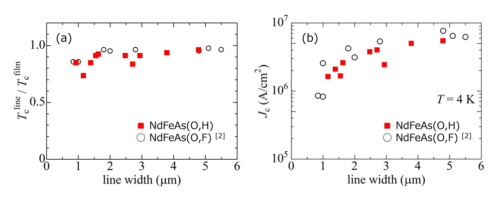
Figure (a) shows the line width dependence of Tc of NdFeAs(O,H) microstrips (red squares). Tc of the strip lines (Tcline) were normalized by that of the film measured before etching (Tcfilm). For comparison, the data of NdFeAs(O,F) microstrips [2] are plotted by black circles. Tcline of NdFeAs(O,H) was generally higher than 85% of Tcfilm down to line width of 1 µm, similarly to NdFeAs(O,F). Figure (b) shows the line width dependence of Jc of NdFeAs(O,H) (red squares) and NdFeAs(O,F) (black circles). It can be seen that there is a decrease in Jc when the line width was 2 µm or less, which was also observed for NdFeAs(O,F). This indicates that the damages caused by the Ar-RIE process was not completely suppressed. Nevertheless, Jc remained high and was more than 1 MA/cm2 down to about 1 µm.
References
[1] C. M. Natarajan et al., Supercond. Sci. Technol. 25, 063001 (2012).
[2] Y. Tsuji et al., Supercond. Sci. Technol. 33, 074001 (2020).
[3] T. Kawaguchi et al., Appl. Phys. Lett. 97, 042509 (2010), T. Kawaguchi et al., Appl. Phys. Express 4, 083102 (2011).
[4] K. Kondo et al., Supercond. Sci. Technol. 33, 09LT01 (2020).
Figures
(a) Normalized Tc and (b) Jc of the strip lines as a function of the line width.
Keywords: iron-based superconductor, microfabrication, photon detector